Making PCBs at home: Milling the first layer (and why you need it)
For the past 5 years I’ve been obsessed about finding a super quick way to make hobby-grade PCBs at home. The race I was looking to win was the “I don’t want to wait 3 weeks being able to do nothing after I remembered that I2C needs in-series resistors”. I want to get my board in my hands in about an hour without doing much.
And I found the way, but most importantly, I found the workflow. Let me show you!
First of all, in case you missed the title, my solution is CNC milling. The upfront cost is quite budget friendly (less than 200 euros), no nasty chemicals are involved and you can safely toss that awfully bad “PCB drill” out the window. The process takes about 30’ of which 5 are manual labor (preparing gcode and toolchanging)
Required tools
While not on the “simple” side, the tools that are required are cheap and can sit on your workbench.
- A CNC. Almost any CNC. If you’re a cheap fuck, a CNC 3018 will cut it (I recommend this). The requirements for the CNC are the following:
- Some way to hold the copper clad safely on the CNC - clamps/screws/whatever
- A 60° 0.1mm-0.2mm endmill to mill the traces (I recommend this set of 10 at 0.2mm)
- A 1mm PCB endmill to cut the board and milldrill (called fishtail? I recommend this set)
- A set of PCB drill bits bellow 1mm (there are many on bg)
- Some single sided copper clad - just make sure it fits on your CNC (source it locally or through bg) The CNC costs ~250 euros and the consumables ~30. You can find even cheaper CNCs but the sainsmart is quite common and has a community. It’s bad as it is (you won’t be cutting aluminum anytime soon) so you definitely want some people to help you. CNCing is generally hard - apart from PCBs, PCBs are easy and hassle free.
Software Preparation
You’re gonna need the following software setup and working:
- pcb2gcode - to generate G-Code from gerbers
- bCNC - G-Code sender that has autoleveling feature
- The gerbers of the board you wanna make - these should have all the traces on the BACK side
Workflow
The whole idea is the following:
- Create gcode from gerbers after some setup (speeds & feeds). The gcode is split in the following files:
- Load
backfile on bCNC - Connect the probe leads to the cutter and the board
- Zero X & Y so that the board fits on the stock and Z roughly 2mm above the board
- Set Z 0 (again) in the origin by going to
Probe tab -> Probe, ConfigurePos: 0, 0, -3and pressProbebutton. The spindle will start going down very slowly until it touches the board. PressZ=0. - Without lifting the Z, go to
Autolevelbutton and press theZerobutton with the crosshairs. - Lift Z to ~5mm and go back to
Probe tab -> Autolevel - Start autolevel probing by:
- Start the cut
- After it’s finished, load the
drillfile WITHOUT saving changes to previous file and WITHOUT deleting the probe mesh (it pops up 2 questions that you should both answer with No) and change the tool - Go to XY origin, wipe a bit the point under the cutter and do a regular probe to set the tool’s offset and set
Z=0after the probe touches - Start the cut
- Repeat steps 10-12 for milldrill and outline
- Profit! To avoid breathing all the fiberglass cut you can have a small syringe filled with water and squirt some as the cuts go. It really helps keep everything super clean.
Another idea is to squirt some WD-40 or cutting fluid during the cut - I haven’t tested it but it sounds pretty good and maybe WD-40 isn’t conductive (so you don’t have to wipe it during probing for tool changes). An idea by James.
Configuring pcb2gcode
pcb2gcode requires some configuration to generate correct G-Code for your setup. This can be done either with a gazillion command line flags or through a file, called millproject that has to be on the same directory that the pcb2gcode command is executed. Here is a thoroughly commented millproject for my machine:
millproject
# Pcb2GCode settings
metric=true # Use mm to read the following values (feeds/speeds/etc.), not imperial inches
metricoutput=true # Same, but for the output
zero-start=true # Start from 0,0,0
zsafe=1 # Safety height
zchange=5 # Height to change a tool - don't over-do it to avoid crushing your Z axis
software=custom # We're not using Mach or LinuxCNC
mirror-axis=1 # Mirror the design to X. Required for the back side
# voronoi=1 # (optional) Instead of cutting straight traces, cut the board only in the places that shouldn't connect with each other. Produces very weird boards but it's quite fast and optimal

# Milling - Trace engraving
zwork=-0.07mm # Depth of engraving - did  quite a lot of testing and it seems 0.07 is quite consistent
mill-feed=600 # How fast to go, in mm/min - maybe go a bit faster?
mill-speed=10000 # How fast to rotate the spindle in RPM
mill-diameters=0.30mm # Caluclated by pcb_mill_calc.py - 0.30mm for 0.2mm 60 degree endmill
isolation-width=0.55mm # Space between traces - I recommend higher than 0.5mm to be MUCH easier to sold and avoid bridges
milling-overlap=20% # How much should the passes to create the isolation width overlap - 20% is good

# Drilling
zdrill=-1.7 # Depth to drill a hole, +0.1mm than the board thickness to have clean holes
zmilldrill=-1.7 # Same but for milldrill
drill-side=back # Drill the board from the back side
drill-feed=25 # Lower Z during drilling at 25mm/s - don't go much higher, CNCs don't like drilling
drill-speed=10000 # How fast to rotate the spindle in RPM
drills-available=0.3mm,0.4mm,0.5mm,0.6mm,0.7mm,0.8mm,0.9mm # Available drill diameters - You "should" have all the diameters smaller than your milldrill bit, if you don't have one it will be rounded to the colsest one you have
milldrill-diameter=1.0mm # Diameter of the milldrill endmill - I suggest 1mm as you have much less toolchanges and it lasts quite long
min-milldrill-hole-diameter=1.0mm # Minimum diameter to milldrill - should be the same with your milldrill diameter

# Outline
zcut=-1.7 # Depth of cut for the outline
cut-side=back # Cut the board from the back
cut-feed=200 # How fast to cut the board in mm/min - can go a LOT faster I think
cut-vertfeed=25 # How fast to plunge into the board - don't go much higher
cut-speed=10000 # How fast to run the spindle in RPM
cut-infeed=0.85 # Do the cutting in multiple passes, 0.85mm each - maybe this isn't needed
cutter-diameter=1.0mm # Diameter of the cutter - use the milldrill bit
bridges=4 # Width of each tab to avoid flying PCBs after the outline is done
bridgesnum=2 # Number of tabs
zbridges=-1.2 # Z height while cutting tabs, -1.2 will result in 0.4mm tabs - 0.4mm is ok

# GRBL shenanigans
# G64 is not supported by GRBL
nog64=true
# https://github.com/gnea/grbl/issues/290
nog81=true
nog91-1=true
While the engraving bit is lets say 0.2mm, you’re cutting 0.07mm lower than the surface so the resulting cut will have a bigger width than 0.2mm. To calculate the effective width of cut I created a python script:
pcb_mill_calc.py
#!/usr/bin/env python3
import math

# For an example of angle=60 tip=0.2 and depth=0.1 check: https://www.calculator.net/right-triangle-calculator.html?av=0.1&alphav=60&alphaunit=d&bv=&betav=&betaunit=d&cv=&hv=&areav=&perimeterv=&x=97&y=22
def calculate_effective_width(angle, tip, depth=0.1):
    rads = math.radians((180-angle)/2)
    return 2 * depth / math.tan(rads) + tip

if __name__ == "__main__":
    import sys

    angle = float(sys.argv[1])
    tip = float(sys.argv[2])
    depth = 0.1
    try:
        depth = float(sys.argv[3])
    except IndexError:
        pass

    print(f"For the tip with {angle} degree angle, {tip}mm tip and for a {depth}mm depth of cut, the following effective width should be used:")
    result = calculate_effective_width(angle, tip, depth)
    recommended = result + (0.05 - (result % 0.05))
    print(f"\t{result} -> rounded up to 0.05mm (for best results): {round(recommended, 2)}")
Usage: python3 pcb_mill_calc.py <bit angle> <bit diameter> <depth of cut>
For example to for my 60° 0.2mm endmill with zwork 0.07mm:
python3 pcb_mill_calc.py 60 0.2 0.07
And I get the following result:
For the tip with 60.0 degree angle, 0.2mm tip and for a 0.07mm depth of cut, the following effective width should be used:
    0.28082903768654766 -> rounded up to 0.05mm (for best results): 0.3
Oof, that’s it! That’s the hardest part but it needs to be done only once - you can then copy the file around in projects and tinker it a bit.
Generate the G-Code
The rest is quite easy, execute the following command:
mkdir -p /tmp/gcode && pcb2gcode \
	--front "/tmp/gerbers/${PROJECT}-CuTop.gbr" \
	--front-output "/tmp/gcode/${PROJECT}-front.ngc" \
	--back "/tmp/gerbers/${PROJECT}-CuBottom.gbr" \
	--back-output "/tmp/gcode/${PROJECT}-back.ngc" \
	--drill "/tmp/gerbers/${PROJECT}.drl" \
	--drill-output "/tmp/gcode/${PROJECT}-drill.ngc" \
	--milldrill-output "/tmp/gcode/${PROJECT}-milldirll.ngc" \
	--outline "/tmp/gerbers/${PROJECT}-EdgeCuts.gbr" \
	--outline-output "/tmp/gcode/${PROJECT}-outline.ngc"
It expects gerbers exported by KiCad (due to the CuTop naming convention and the rest) to be under /tmp/gerbers and a variable PROJECT with the name of the KiCad project. If you have indeed a KiCad project, I have an even better command that using KiKit, generates the gerbers and feeds them to pcb2gcode automatically:
export PROJECT=${$(ls *.kicad_pcb)%.kicad_pcb} && \
	kikit export gerber "${PROJECT}.kicad_pcb" /tmp/gerbers && \
	mkdir -p /tmp/gcode && \
	pcb2gcode \
	--front "/tmp/gerbers/${PROJECT}-CuTop.gbr" \
	--front-output "/tmp/gcode/${PROJECT}-front.ngc" \
	--back "/tmp/gerbers/${PROJECT}-CuBottom.gbr" \
	--back-output "/tmp/gcode/${PROJECT}-back.ngc" \
	--drill "/tmp/gerbers/${PROJECT}.drl" \
	--drill-output "/tmp/gcode/${PROJECT}-drill.ngc" \
	--milldrill-output "/tmp/gcode/${PROJECT}-milldirll.ngc" \
	--outline "/tmp/gerbers/${PROJECT}-EdgeCuts.gbr" \
	--outline-output "/tmp/gcode/${PROJECT}-outline.ngc"
Continue to Step 2 from Workflow and you’ll be done in minutes!
The End
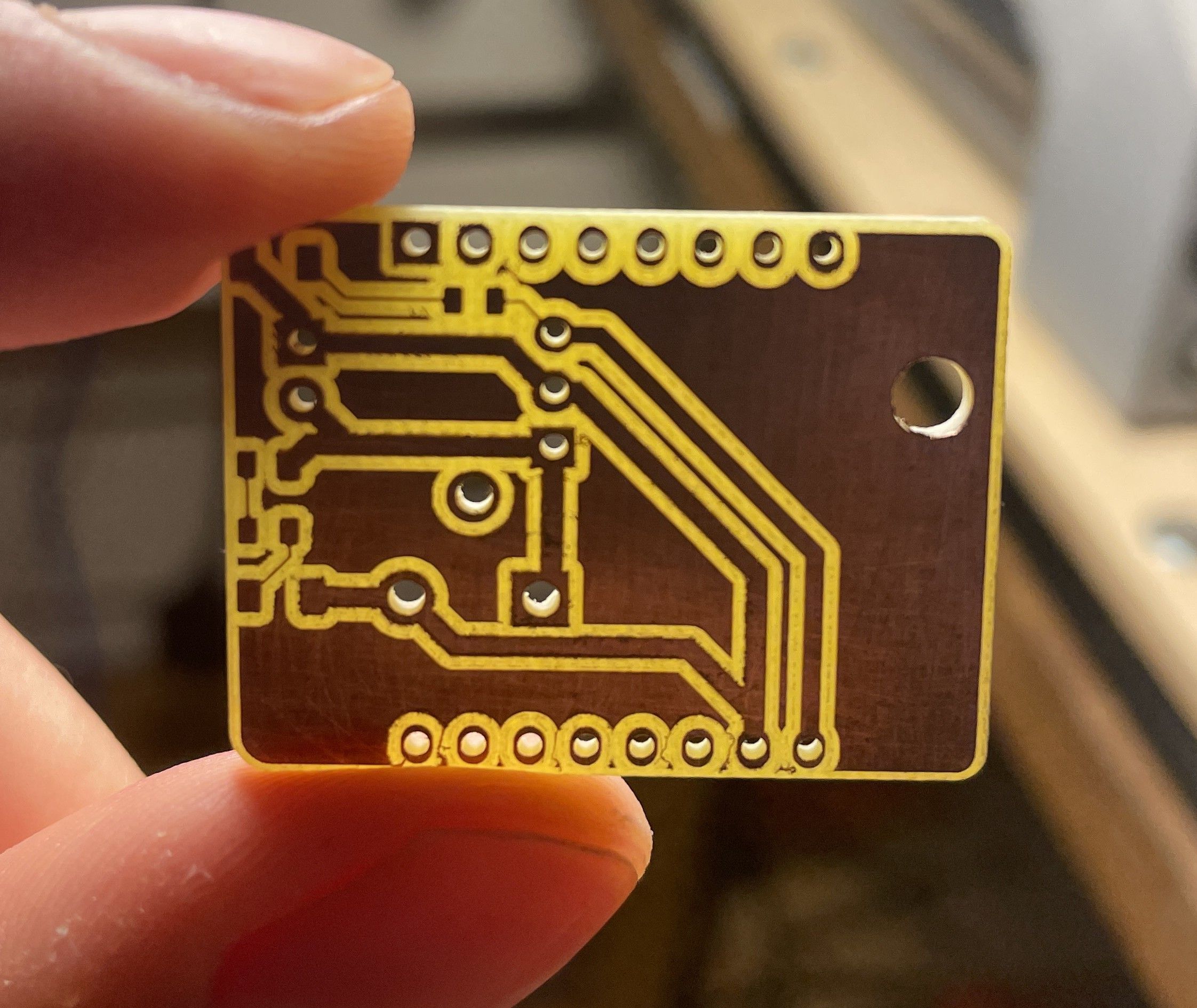
This was quite a journey for me and it took me about 2 years to finish this workflow. Takes about 30’ to make a small board, it’s almost free. The cutters don’t wear much, copper clads are dirt cheap and widely available even in local stores. The boards turn out amazingly well with almost no post-processing required - maybe some flying copper hair.
I’m already preparing the workflow for a double sided PCB workflow, most probably using a spindle camera (it’s cheap, don’t freak out). Stay tuned.
What I haven’t figured out is how to apply solder mask. It needs a weird spring-loaded tool that is able to remove 0.01-0.02 material. If you have any cool ideas, leave a comment!
Alternative PCB making methods
This is a list on ways to make PCBs at home and why I chose milling over everything else:
- Toner transfer with iron
- Plotter marker (have a plotter with a permanent marker on bare copper clad, there’s an awesome guide by Stavros here)
- Laser engraver (Photosensitive board that is marked by the laser)
- CNC Milling
Troubleshooting
I wanna keep this section up-to-date with problems that I stumble upon. If you have any problems, even machine-specific, please leave a comment.
Even after leveling, I get uneven traces that are too deep or shallow
First of all, make sure that you didn’t press the small Autolevel button. What this does is apply the autolevel offsets a second time so the result is just like if you hadn’t leveled your workpiece - but from the opposite side
Then, check that your probe wire doesn’t pick up noise from the motors or spindle. You can check this but doing some movement with your machine and watching if a [P] will randomly show in the machine status. If you have this problem read Grbl Wiki on the matter. Based on that I’ve created this board that has 4 optocouplers to isolate the limit switch circuit from the rest of the controller. Worked wanders for me